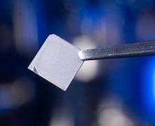
Thin films, defined as thin layers of material with thicknesses typically measured in nanometers or micrometers, are crucial in numerous scientific and industrial applications. The preparation and characterization of these films involve a range of techniques and considerations.
Several methods are employed for the preparation of thin films, each with its own set of advantages and applications. Physical vapor deposition (PVD) techniques, such as sputtering and evaporation, involve transferring material from a source to a substrate in a vacuum environment. Chemical vapor deposition (CVD) methods, on the other hand, use chemical reactions to deposit material onto a substrate. These reactions can be thermal, photochemical, or plasma-enhanced, allowing for the deposition of a wide range of materials.
Electrochemical deposition, also known as electrodeposition, is another commonly used method for preparing thin films. This technique involves applying an electrical potential to a substrate immersed in an electrolyte solution, causing ions to be reduced or oxidized at the electrode surface and form a film. Sol-gel methods and molecular beam epitaxy (MBE) are additional preparation techniques, offering high precision and control over the composition and structure of thin films.
The characterization of thin films is essential for understanding their properties and performance. Techniques such as X-ray diffraction (XRD) and electron diffraction are used to determine the crystallinity and structure of thin films. Scanning electron microscopy (SEM) and atomic force microscopy (AFM) provide high-resolution images of the film’s surface and interface, revealing topographical features and defects.
Optical spectroscopy techniques, including spectrophotometry and ellipsometry, are used to measure the optical properties of thin films, such as transmittance, reflectance, and absorption. These measurements are crucial for applications in optics and photonics. Electrical characterization techniques, such as Hall effect measurements and four-point probe tests, are used to determine the electrical properties of thin films, including conductivity, resistivity, and carrier concentration.
The preparation and characterization of thin films are closely linked to their potential applications. For instance, superconducting thin films require precise control over their composition and structure to achieve high critical temperatures and current densities. Conductive thin films must exhibit high conductivity and transparency for applications in displays and solar cells. Ferroelectric thin films require well-defined crystallographic orientations for optimal performance in memory devices and sensors.
In conclusion, the preparation and characterization of thin films are complex processes involving a range of techniques and considerations. The ability to precisely control the composition, structure, and properties of these films is crucial for their application in various scientific and industrial fields. As technology continues to advance, we can expect to see even more sophisticated methods for the preparation and characterization of thin films, enabling the development of new materials and applications.