Thin films, often referred to as “Thin Film” in the realm of materials science, represent a vital component in numerous industries and scientific domains. These extremely thin layers of material, though minimal in thickness, exhibit unique physical, chemical, and electrical properties that make them indispensable. This article delves into the diverse applications of thin films and the techniques employed in their growth.
Applications of Thin Films
- Superconducting Thin Films
- Deposited using methods like evaporation and sputtering, superconducting thin films have thicknesses less than 1 micrometer.
- They are pivotal in creating digital circuits that outperform those made from semiconductor materials, offering faster speeds, lower losses, and higher capacities.
- Microwave communication devices like antennas, resonators, filters, and delay lines crafted from superconducting thin films exhibit unparalleled sensitivity, making them a highly valued material in electronic warfare.
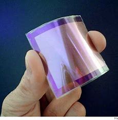
- Conductive Thin Films
- Conductive thin films encompass both semi-conducting and conducting materials.
- Transparent conductive thin films, which can conduct electricity while maintaining high transparency within the visible light spectrum, find applications in liquid crystal displays (LCDs), solar cells, and various optical fields.
- Materials like indium tin oxide (ITO) are extensively researched for their conductive and transparent properties.
- Ferroelectric Thin Films
- Ferroelectric thin films, with thicknesses ranging from tens of nanometers to a few micrometers, exhibit ferroelectricity.
- They possess excellent ferroelectric, piezoelectric, pyroelectric, electrical, and nonlinear optical properties.
- These films are crucial in microelectronics, optoelectronics, integrated optics, and micro-electromechanical systems (MEMS), primarily used in manufacturing memory devices, sensors, transducers, and optical devices.
Techniques for Thin Film Growth
- Physical Vapor Deposition (PVD)
- A versatile technique that can be used to deposit films of almost any material.
- Methods within PVD include thermal evaporation, sputtering, and pulsed laser deposition.
- Sputtering involves bombarding a solid target with high-energy ions, causing atoms to be ejected and deposited on a substrate to form a thin film.
- Pulsed laser deposition uses a high-power pulsed laser to vaporize the target material, forming a plasma plume that condenses on the substrate.
- Chemical Vapor Deposition (CVD)
- A chemical technique used to produce high-purity, high-performance solid materials.
- In CVD, a substrate is exposed to one or more precursor gases, which undergo chemical reactions on the substrate surface to form the desired thin film.
- Variants of CVD include Atmospheric Pressure CVD (APCVD), Low-pressure CVD (LPCVD), Ultrahigh vacuum CVD (UHVCVD), Aerosol-assisted CVD (AACVD), and Direct Liquid Injection CVD (DLICVD), each tailored for specific applications and material properties.
In conclusion, thin films occupy a pivotal position in modern technology, thanks to their diverse applications and the sophisticated techniques used to grow them. From superconducting films that revolutionize digital circuits to ferroelectric films that enhance the functionality of electronic devices, thin films continue to push the boundaries of what is possible. As research progresses, we anticipate even more innovative applications and techniques, further cementing the role of thin films in shaping our technological future.