Thin films are thin layers of material with thicknesses ranging from a few nanometers to a few micrometers. They are widely used in various industries due to their unique properties and applications. This article delves into the science and technology behind thin films.
1. Preparation Techniques
There are several methods for preparing thin films, including physical vapor deposition (PVD), chemical vapor deposition (CVD), electrochemical deposition, sol-gel processing, and molecular beam epitaxy (MBE). Each method has its own advantages and disadvantages, and the choice of method depends on the specific requirements of the application.
PVD involves depositing material from a solid source onto a substrate in a vacuum. CVD, on the other hand, involves the reaction of gaseous precursors to form a solid film on a substrate. Electrochemical deposition involves the use of an electrical current to deposit material onto a substrate from a solution. Sol-gel processing involves the formation of a gel from a solution, followed by drying and sintering to form a thin film. MBE is a high-vacuum technique used to deposit single-crystal films with atomic-scale precision.
2. Properties of Thin Films
Thin films exhibit distinct physical, chemical, and electrical properties compared to their bulk counterparts. These properties are influenced by factors such as film thickness, composition, structure, and defects. For example, thin films can be single-crystalline, polycrystalline, or amorphous, and their properties will vary accordingly.
Thin films also exhibit size effects, where the properties of the film depend on its dimensions. This is due to the confinement of electrons, phonons, and other excitations within the film. Additionally, thin films can exhibit surface and interface effects, where the properties of the film are influenced by its interactions with the substrate and the surrounding environment.
3. Applications of Thin Films
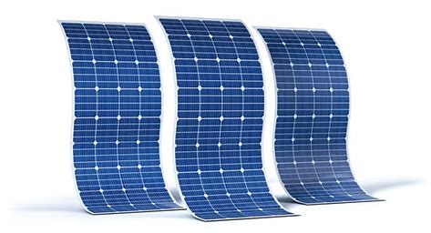
Thin films have a wide range of applications in various industries. In electronics, they are used in integrated circuits, microwave communication devices, and sensors. In optics, they are used in reflective coatings, anti-reflection coatings, and filters. Thin films are also used in solar energy conversion, particularly in solar cells, where they play a crucial role in converting sunlight into electricity.
Additionally, thin films are used in biomedical devices, coatings for corrosion resistance, and more. For example, thin films of titanium nitride are used as wear-resistant coatings on cutting tools and medical implants. Thin films of zinc oxide are used in varistor devices, which are used in surge protection circuits.
4. Challenges and Future Directions
Despite their wide range of applications, thin films face several challenges. One of the main challenges is the control of film thickness and composition, which can affect the properties and performance of the film. Additionally, the scalability of thin film preparation techniques is another challenge, particularly for large-scale applications.
Future research in thin films will focus on developing new preparation techniques that can overcome these challenges and expand the applications of thin films. This includes the development of new materials, such as two-dimensional materials and topological insulators, which have unique properties that make them ideal for various applications. Additionally, research will focus on improving the performance and stability of thin films, as well as exploring new applications in emerging fields such as quantum computing and energy harvesting.
In conclusion, thin films are an essential part of modern technology, with a wide range of applications in various industries. Understanding the science and technology behind thin films is crucial for their continued development and expansion into new fields.